ShiftRow and InvShiftRow change the order of bytes within a 16 byte (128
bit) word. Both transformations involve only changing the order of
signals, and therefore they can be implemented using routing only, and
do not require any logic resources, such as Configurable Logic Blocks
(CLBs) or dedicated RAM. MixColumn / InvMixColumn influences usually the
cipher area very much. Therefore, we proceeded further with the
resource sharing for these blocks. In order to significantly decrease
the area of MixColumn / InvMixColumn , a joint implementation described
in detail in the Ref. [19] is proposed in Fig. 5. The four inputs and
four outputs represent single bytes. Four identical blocks like that one
shown in Fig. 5, constitute the MixColumn block diagram. KeyAddition is
a bitwise XOR of two 128 bit words. The implementation of the
encryption and decryption combined unit is shown in Fig. 6. It requires
realization of five component operations: Substitution , ShiftRow ,
InvShiftRow , MixColumn , and KeyAddition . The values of the selection
signals selEncDec , selData , selMode , and selReg for the multiplexers
are also described. The architecture shown in Fig. 6 is very compact and
is based on the resource sharing for two blocks Substitution and
MixColumn in order to achieve minimum area of the circuit. It has been
proven from simulations and further on from implementation that by using
the resource sharing of these blocks the area of the circuit is with
16% less. ShiftRow and InvShiftRow do not require any logic resources in
FPGA implementation. The Rijndael cipher in OCB/ECB modes of operation
was first described in Verilog, and his description verified using the
Verilog-XL simulator from Cadence Design Systems. Test vectors from the
reference software implementations were used for debugging and
verification of Verilog codes. The revised Verilog code became an input
to Xilinx ISE Series 4.1 i software performing the logic synthesis,
mapping, placing, and routing. In order to fit the whole circuit in one
FPGA device Virtex II XC2V1000-4, the option for the Xilinx ISE Series
4.1 i software was set to small area and the design has been flatten.
These tools generated reports describing the area and speed of
implementation, a netlist used for timing simulations, and a bitstream
to be used to program the FPGA device Virtex II XC2V1000-4 [22]. The
software [23] used to provide test vectors for OCB mode of operation was
written in C and C CC and is available at Rogaway’s home page. The test
vectors as well as the variables of a pipeline with five inputs ( n Z 5
in Fig. 3) containing 74 blocks of data encrypted in OCB are
represented in Fig. 7. For simplicity, key, nonce, and plaintext are all
set to zero. The timing simulation results of the test vectors were
performed with the key KeyIn [0:15] and the input Input [0:15] set to
zero, as shown in Fig. 8. ModeOperation and EncDec are ‘1/0’ logic for
OCB/ECB and encryption/ decryption, respectively. Length [4:0] shows the
number of remaining blocks of data and Counter [11:0] displays the
number of packages. The maximum number of packages transmitted in WLANs
is 4095 and therefore 12 bits are needed for coding. NewKey is ‘1’ logic
whenever is desired to load an external key. The reset of the circuit
is synchronous through reset while start and done are part of the
handshaking protocol. In order to program the FPGA, a SUN workstation
was connected to the Insight Virtex II Development Kit board [24]. The
board was connected to the Logic Analysis System Agilent 16702B [25]
which provided and displayed signals during measurements. The
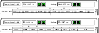
experimental results are shown in Fig. 9. The results of the FPGA
implementation are summarized in Table 1. The throughput of the circuit
in OCB mode is given by:


No comments:
Post a Comment